p-channel mosfet.
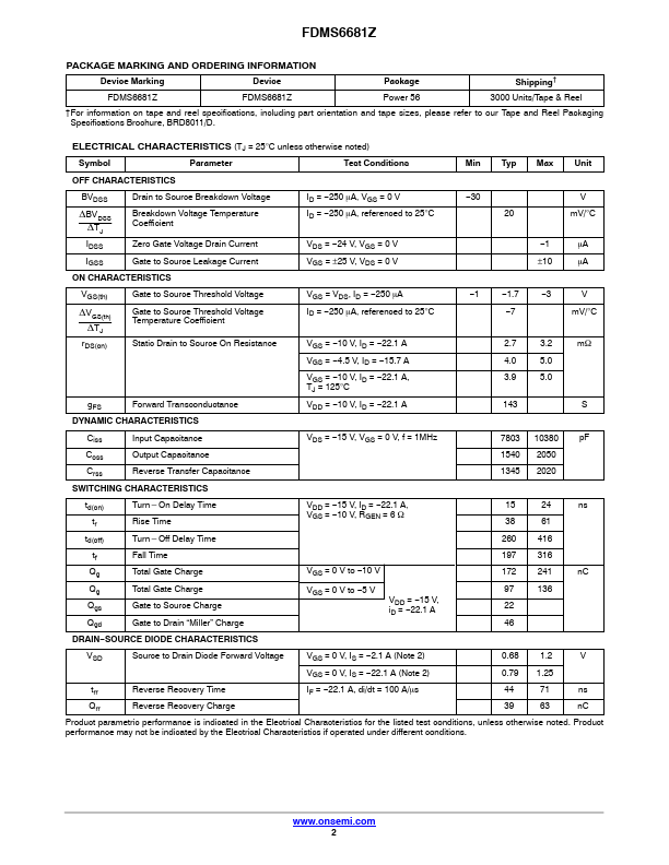
* Max rDS(on) = 3.2 mW at VGS = −10 V, ID = −21.1 A
* Max rDS(on) = 5.0 mW at VGS = −4.5 V, ID = −15.7 A
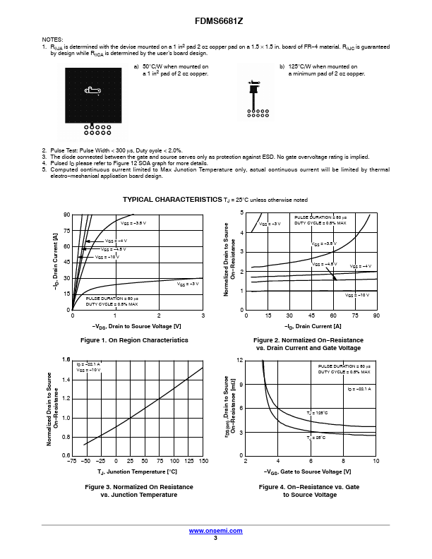
* Advanced Package and Silicon Combination for Low rD.
Advancements in both silicon and package technologies have been combined to offer the lowest rDS(on) and ESD protection.
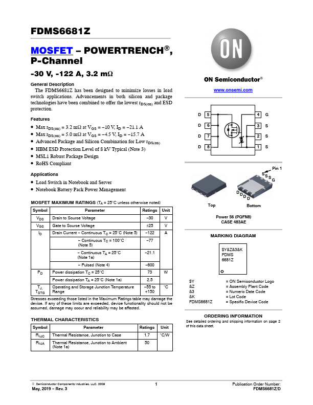
The FDMS6681Z has been designed to minimize losses in load
switch applications. Advancements in both silicon and package technologies have been combined to offer the lowest rDS(on) and ESD protection.
Features
* Max rDS(on) = 3.2 mW at VGS = −10 .
Image gallery
TAGS
Manufacturer
Related datasheet
 Download (Size : 374.82KB)